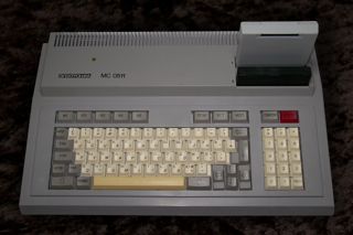
PDP-11 for the UKNC
The UKNC is a Russian home computer.
Intended for educational purposes, it's CPUs are a direct copy of
the PDP-11 processor.
The UKNC actually uses Two PDP-11 processors, one for the main CPU,
one for the 'Peripheral processor'... the CPU runs the main code...
the PP handles Keyboard, Disk and graphics - though the main CPU can
directly access 2 of the 3 graphics bitplanes (It can't access all 3
|
 |

|

|
| Cpu |
KM181VM2 (PDP-11 Compatible)
Main: 8mhz PP: 6.25mhz |
| Ram |
Main: 64k PP: 32k |
| Vram |
2k |
| Resolution |
up to 640x288 @ 8 colors |
| Sprites |
|
| Tilemap |
|
| Colors |
4 (2 bitplane) or 8 (4 bitplane) from a palette of 15 |
| Sound chip |
|
|
 |
Emulator
UKNC BTL - Best (or
only) Emulator for the UKNC
ChibiAkumas Tutorials
Useful Documentation
Ansi
Escape Codes (VT100 Terminal)
Video Ports
Function
|
From CPU
|
From PPU
|
Select Address
|
177640 |
177010 |
Write Plane 0 (Blue)
|
(impossible) |
177012 |
Write Plane 1 (Green)
|
176642 |
177014 |
Write Plane 2 (Red)
|
176643 |
177015 |
CPU RAM
| From |
To |
Purpose |
| 0 |
157777 |
RAM |
| 160000 |
177777 |
IO |
PPU RAM
| From |
To |
Purpose |
| 0 |
77777 |
RAM |
| 100000 |
117777 |
RAM Window |
| 120000 |
176777 |
ROM |
| 177000 |
177777 |
IO |
UKNC Color Palette
0
|
1
|
2
|
3
|
4
|
5
|
6
|
7
|
8
|
9
|
A
|
B
|
C
|
D
|
E
|
F
|
UKNC
CPU Ports
| 60 |
CH0 IN Interrupt |
Channel 0 |
| 64 |
CH0 OUT Interrupt |
Channel 0 |
| 460 |
CH1 IN Interrupt |
Channel 1 |
| 464 |
CH1 OUT Interrupt |
Channel 1 |
| 474 |
CH2 OUT Interrupt |
Channel 2 |
| 176000 |
Windows Register |
|
| 176000 |
Window A register |
|
| 176001 |
Window B register |
|
| 176640 |
Bitplanes address register (RA) |
|
| 176642 |
Write Plane 1 (Green) (RD) |
|
| 176643 |
Write Plane 2 (Red) (RD) |
|
| 176660 |
C1 in STATUS |
Channel 1 |
| 176662 |
C1 in DATA |
Channel 1 |
| 176664 |
C1 out STATUS |
Channel 1 |
| 176666 |
C1 out DATA |
Channel 1 |
| 176674 |
C2 out STATUS |
Channel 2 |
| 176676 |
C2 out DATA |
Channel 2 |
| 177560 |
C0 Console in STATUS |
Channel 0 |
| 177562 |
C0 Console in DATA |
Channel 0 |
| 177564 |
C0 Console out STATUS |
Channel 0 |
| 177566 |
C0 Console out DATA |
Channel 0 |
UKNC
PP Ports
| 300 |
Keyboard interrupt vector |
|
| 304 |
Programmable timer interrupt |
|
| 310 |
External event interrupt |
|
| 314 |
;RESET on CPU bus interrupt |
|
| 320 |
CH0 IN Interrupt |
Channel 0 |
| 324 |
CH0 OUT Interrupt |
Channel 1 |
| 330 |
CH1 IN Interrupt |
Channel 1 |
| 334 |
CH1 OUT Interrupt |
Channel 2 |
| 340 |
CH2 IN Interrupt |
Channel 2 |
| 177010 |
Bitplanes address register (RA) |
|
| 177012 |
Write Plane 0 (Blue) (RD) |
|
| 177014 |
Write Plane 1 (Green) (RD) |
|
| 177015 |
Write Plane 2 (Red) (RD) |
|
| 177016 |
PPU dots color |
|
| 177020 |
PPU bitplanes 0/1 background color |
|
| 177022 |
PPU bitplanes 1/2 background color |
|
| 177024 |
PPU dots octet |
|
| 177026 |
PPU bitplanes mask register |
|
| 177054 |
Window (100000-117777) |
|
| 177060 |
C0 in DATA |
Channel 0 |
| 177062 |
C1 in DATA |
Channel 1 |
| 177064 |
C1 in DATA |
Channel 2 |
| 177066 |
C0 in STATUS |
Channel 0 |
| 177066 |
C1 in STATUS |
Channel 1 |
| 177066 |
C2 in STATUS |
Channel 2 |
| 177070 |
C0 out DATA |
Channel 0 |
| 177072 |
C1 out DATA |
Channel 1 |
| 177076 |
C0 out STATUS |
Channel 0 |
| 177076 |
C1 out STATUS |
Channel 1 |
| 177320 |
Joystick "Diana", etc. |
|
| 177700 |
Keyboard state register |
|
| 177702 |
Keyboard data register |
|
| 177710 |
State register |
DI------
D=Data Waiting (1=Yes) I=Interrupts Enabled(1=on)
|
| 177712 |
Buffer register |
SKKKKKKK S=State(0=pressed 1=released)
K=Keycode 0-127 (0-15 when released - parital only) |
| 177714 |
Current state register |
|
| 177716 |
System control register - Bit 7 - Beeper |
|
UKNC
RAM
and VRAM
The UKNC has 192K total split into 3 banks.
The top 32k is used for VRAM, The top 32k of Bank 0 makes up the 'Blue'
bitplane, The top 32k of Bank 1 makes up the 'Green' bitplane, The top 32k
of Bank 2 makes up the 'Red' bitplane.
The bottom 32k is used by one of the two CPU's
The 32k of banks 1+2 are combined to make up the 64k ram used by the Main
CPU (the one that runs our program)... bytes from Bank 1 are at Even
Addresses, Bytes from Bank 2 are at Odd addresses of the Main CPU ram.
The 32k of Bank 0 makes up the 32k Low area of the Peripheral Processor
(PP) Sub CPU (the top 32k is rom).
There is no way to 'swap' these ram banks via bankswitching, however the
CPU's can access the VRAM, and the Peripheral Processor 'PP' Sub CPU can
access the Main CPU's ram via the 'RAP' device.
The RAP device is a third chip which has complete access to all the
memory, we select an address with one port, then write data with the other
two or three (depending on CPU - the SUB PP CPU can access all 3, the main
CPU can access only 2)... this is how we typically write to VRAM.
It is also possible to re-configure the SLTAB line table, and move the
visible RAM into an area the CPU's can directly access, however this will
reduce the RAM available for other purposes.
Physical addresses and
RAP ports
CPU RAP Address select port: 176640
PP RAP Address select port : 177012
|
Physical
Addresses |
|
Bank 0
Blue VRAM
|
Bank 1
Green VRAM |
Bank 2
Red VRAM |
Used for VRAM
by default |
177777 |
177777 |
177777 |
| ...... |
...... |
...... |
| 100001 |
100001 |
100001 |
| 100000 |
100000 |
100000 |
Used for RAM
by default |
077777 |
077777 |
077777 |
| ...... |
...... |
...... |
| 000001 |
000001 |
000001 |
| 000000 |
000000 |
000000 |
RAP
MAIN CPU Port
|
Impossible
|
176642
|
176643
|
| RAP
PP CPU Port |
177012 |
177014 |
177015 |
Main CPU Memory
assignment
Bytes from Banks 1+2 make alternate bytes of CPU ram
| Main CPU Address |
RAM
Even Add |
RAM
Odd Addr |
|
177776/177777 |
077777 |
077777 |
|
............. |
...... |
...... |
|
100002/100003 |
040001 |
040001 |
|
100000/100001 |
040000 |
040000 |
|
077776/077777 |
037777 |
037777 |
|
............. |
...... |
...... |
|
000002/000003 |
000001 |
000001 |
|
000000/000001 |
000000 |
000000 |
Sub CPU PP Memory
assignment
Low 32k uses Bank 0 RAM (both odd and even), High 32k uses ROM (both odd
and even)
Sub CPU
PP address |
ROM
(Odd and Even) |
RAM
(Odd and Even) |
|
177776/177777 |
077776/077777 |
|
|
............. |
............. |
|
|
100002/100003 |
000002/000003 |
|
|
100000/100001 |
000000/000001 |
|
|
077776/077777 |
|
077776/077777 |
|
............. |
|
............. |
|
000002/000003 |
|
000002/000003 |
|
000000/000001 |
|
000000/000001 |
UKNC
SLTAB
entries
*** Thanks to aberrant_hacker for this
information on the UKNC!... he's working on a port of ChibiAkumas to the
UKNC... check it out here!
***
The STAB is the line definition table, it
starts at address 270, each line has two words, the first is the VRAM
address of that line, the second is a pointer to the next line, and a few
options... more options can be configured using a 4 word SLTAB definition.
There are 3 types of record, one uses 2 words
per record, the other two use 4 words... what record is next is defined by
the L and S bits of the previous line.
312 (1..312) lines is SECAM half-frame
309 (1..309) SLTAB records in total (lines 4..312 of SECAM's half-frame)
scanlines 1..19 are not visible due to the
vertical blanking interval
scanlines 20..307 are visible (lines 23-310 of SECAM's
half-frame)
scanlines 308..309 are not visible due to the vertical blanking
interval
|
F |
E |
D |
C |
B |
A |
9 |
8 |
7 |
6 |
5 |
4 |
3 |
2 |
1 |
0 |
|
2 word
record |
V |
V |
V |
V |
V |
V |
V |
V |
V |
V |
V |
V |
V |
V |
V |
V |
V=Vram Address |
| A |
A |
A |
A |
A |
A |
A |
A |
A |
A |
A |
A |
A |
S |
L |
C |
C=Toggle Cursor on/off L=Length
of next record (2/4 words)
S= 4-word selector
(Options/Palette) / 2-word address bit 2 A=Address
bits 3-15 |
|
F |
E |
D |
C |
B |
A |
9 |
8 |
7 |
6 |
5 |
4 |
3 |
2 |
1 |
0 |
|
4 word
record
Options |
- |
C |
C |
C |
C |
C |
C |
C |
G |
G |
G |
T |
Y |
R |
G |
B |
YRGB=Cursor
color & Brightness / T=Type
(Char/Graphic) / G=Graphic
Cursor pos / C=Cursor pos |
| - |
- |
- |
- |
- |
- |
- |
- |
- |
- |
S |
S |
- |
R |
G |
B |
RGB=
Line Brightness S=Scale
(640/320/160/80) |
| V |
V |
V |
V |
V |
V |
V |
V |
V |
V |
V |
V |
V |
V |
V |
V |
V=Vram Address |
| A |
A |
A |
A |
A |
A |
A |
A |
A |
A |
A |
A |
A |
S |
L |
C |
C=Toggle Cursor on/off L=Length
of next record (2/4 words)
S= 4-word selector
(Options/Palette) / 2-word address bit 2 A=Address
bits 3-15 |
|
F |
E |
D |
C |
B |
A |
9 |
8 |
7 |
6 |
5 |
4 |
3 |
2 |
1 |
0 |
|
4 word
record
palette |
Y |
R |
G |
B |
Y |
R |
G |
B |
Y |
R |
G |
B |
Y |
R |
G |
B |
Palette
bit combos %011 %010 %001 %001 |
| Y |
R |
G |
B |
Y |
R |
G |
B |
Y |
R |
G |
B |
Y |
R |
G |
B |
Palette
bit combos %111 %110 %101 %100 |
| V |
V |
V |
V |
V |
V |
V |
V |
V |
V |
V |
V |
V |
V |
V |
V |
V=Vram Address |
| A |
A |
A |
A |
A |
A |
A |
A |
A |
A |
A |
A |
A |
S |
L |
C |
C=Toggle Cursor on/off L=Length
of next record (2/4 words)
S= 4-word selector
(Options/Palette) / 2-word address bit 2 A=Address
bits 3-15 |
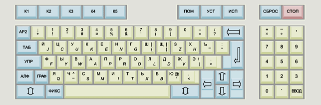
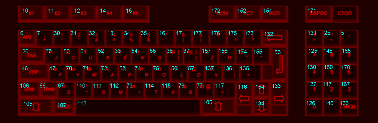
UKNC Keyboard Scancodes
We can read the keyboard only from the PPU, The best way is by
writing our own Keyboard interrupt handler, and copying it's address
to memory address #300 in octal... This will cause it to execute
each time a key is pressed or released.
We can then read port 177702 to get the details of the key that was
pressed.
Bit 7 will be zero if a key was pressed down... Bits 0-6 will give
the full keycode of the key pressed down.
Bit 7 will be 1 if a key was released up... Bits 0-3 will give the
partial keycode of the key released - this means it is not possible
to 100% uniquely identify the key that was released. |
| Bits |
7
|
6
|
5
|
4
|
3
|
2
|
1
|
0
|
| KeyDown |
0 |
K |
K |
K |
K |
K |
K |
K |
| KeyUp |
1 |
0 |
0 |
0 |
K |
K |
K |
K |
|
| Octal |
Decimal |
Hexadecimal |
key |
Details |
| 5 |
5 |
05 |
, |
NumPad |
| 6 |
6 |
06 |
АР2 |
Esc |
| 7 |
7 |
07 |
; / + |
|
| 10 |
8 |
08 |
К1 / К6 |
F1 / F6 |
| 11 |
9 |
09 |
К2 / К7 |
F2 / F7 |
| 12 |
10 |
0A |
КЗ / К8 |
F3 / F8 |
| 13 |
11 |
0B |
4 / � |
|
| 14 |
12 |
0C |
К4 / К9 |
F4 / F9 |
| 15 |
13 |
0D |
К5 / К10 |
F5 / F10 |
| 16 |
14 |
0E |
7 / ' |
|
| 17 |
15 |
0F |
8 / ( |
|
| 25 |
21 |
15 |
- |
NumPad |
| 26 |
22 |
16 |
ТАБ |
Tab |
| 27 |
23 |
17 |
Й / J |
|
| 30 |
24 |
18 |
1 / ! |
|
| 31 |
25 |
19 |
2 / " |
|
| 32 |
26 |
1A |
3 / # |
|
| 33 |
27 |
1B |
Е / E |
|
| 34 |
28 |
1C |
5 / % |
|
| 35 |
29 |
1D |
6 / & |
|
| 36 |
30 |
1E |
Ш / [ |
|
| 37 |
31 |
1F |
Щ / ] |
|
| 46 |
38 |
26 |
УПР |
Ctrl |
| 47 |
39 |
27 |
Ф / F |
|
| 50 |
40 |
28 |
Ц / C |
|
| 51 |
41 |
29 |
У / U |
|
| 52 |
42 |
2A |
К / K |
|
| 53 |
43 |
2B |
П / P |
|
| 54 |
44 |
2C |
H / N |
|
| 55 |
45 |
2D |
Г / G |
|
| 56 |
46 |
2E |
Л / L |
|
| 57 |
47 |
2F |
Д / D |
|
| 66 |
54 |
36 |
ГРАФ |
Graph |
| 67 |
55 |
37 |
Я / Q |
|
| 70 |
56 |
38 |
Ы / Y |
|
| 71 |
57 |
39 |
В / W |
|
| 72 |
58 |
3A |
А / A |
|
| 73 |
59 |
3B |
И / I |
|
| 74 |
60 |
3C |
Р / R |
|
| 75 |
61 |
3D |
О / O |
|
| 76 |
62 |
3E |
Б / B |
|
| 77 |
63 |
3F |
Ю / @ |
|
| 105 |
69 |
45 |
HP |
Shift |
| 106 |
70 |
46 |
АЛФ |
CapsLock |
| 107 |
71 |
47 |
ФИКС |
Lock |
| 110 |
72 |
48 |
Ч / ^ |
|
| 111 |
73 |
49 |
С / S |
|
| 112 |
74 |
4A |
М / M |
|
| 113 |
75 |
4B |
SPACE |
Space
|
| 114 |
76 |
4C |
Т / T |
|
| 115 |
77 |
4D |
Ь / X |
|
| 116 |
78 |
4E |
← |
Left |
| 117 |
79 |
4F |
, / < |
|
| 125 |
85 |
55 |
7 |
NumPad |
| 126 |
86 |
56 |
0 |
NumPad |
| 127 |
87 |
57 |
1 |
NumPad |
| 130 |
88 |
58 |
4 |
NumPad |
| 131 |
89 |
59 |
+ |
NumPad |
| 132 |
90 |
5A |
ЗБ |
Backspace |
| 133 |
91 |
5B |
→ |
Right |
| 134 |
92 |
5C |
↓ |
Down |
| 135 |
93 |
5D |
. / > |
|
| 136 |
94 |
5E |
Э / \ |
|
| 137 |
95 |
5F |
Ж / V |
|
| 145 |
101 |
65 |
8 |
NumPad |
| 146 |
102 |
66 |
. |
NumPad |
| 147 |
103 |
67 |
2 |
NumPad |
| 150 |
104 |
68 |
5 |
NumPad |
| 151 |
105 |
69 |
ИСП |
Execute |
| 152 |
106 |
6A |
УСТ |
Settings |
| 153 |
107 |
6B |
ВВОД |
Enter |
| 154 |
108 |
6C |
↑ |
Up |
| 155 |
109 |
6D |
: / * |
|
| 156 |
110 |
6E |
Х / H |
|
| 157 |
111 |
6F |
З / Z |
|
| 165 |
117 |
75 |
9 |
NumPad |
| 166 |
118 |
76 |
ВВОД |
NumPad |
| 167 |
119 |
77 |
3 |
NumPad |
| 170 |
120 |
78 |
6 |
NumPad |
| 171 |
121 |
79 |
СБРОС |
Reset |
| 172 |
122 |
7A |
ПОМ |
Help |
| 173 |
123 |
7B |
/ / ? |
|
| 174 |
124 |
7C |
Ъ / } |
|
| 175 |
125 |
7D |
- / = |
|
| 176 |
126 |
7E |
О / } |
|
| 177 |
127 |
7F |
9 / ) |
|
