6809 Assembly programming for the Dragon 32/64 and Tandy COCO

The Dragon is an odd beast! Using the impressive 6809 CPU, it somehow ends up being no better than it's 6502 competitors... part of the reason for this is it's clocked at less than 1mhz, and part is the limited RAM and Graphics of the system.

The Dragon 32/64 are virtually the same machine, and strangely, the Tandy COCO (TRS-80 COLOR) is also 99% compatible, for this reason we'll be covering them both here.

For simplicity, In these tutorials, we'll be looking at 32k systems, we won't cover the 4k/16k COCO


Dragon 32 Dragon 64 Tandy COCO (TRS-80 Color Computer)
Cpu 0.89mhz 6809
0.89mhz 6809 0.89mhz 6809
Ram 32k  64k 4k/16k/32k/64k
Max Resolution 128x192 @ 4 color (6k)
256x192 @ 2 color (6k)
128x192 @ 4 color (6k)
256x192 @ 2 color (6k)
128x192 @ 4 color (6k)
256x192 @ 2 color (6k)
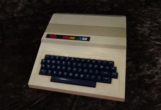
Dragon 32
I am Dragon , hear me roar... Gao!

ChibiAkumas Dragon/CoCo Tutorials

Lesson P1 - Keyboard and Joystick reading on the Dragon / CoCo [DGN]
Lesson P4 - Bitmap Drawing on the Dragon / Tandy CoCo [DGN]
Lesson P8 - Sound on the Dragon / Tandy CoCo [DGN]
Lesson P9 - 16 color Bitmap Drawing on the TRS-80 CoCo 3 [CCO]

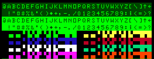
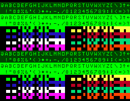
Character Map
Text characters + Semigraphics
 

Screen Modes

The Dragon has a variety of possible modes... the most useful being the 'Full Graphics' modes...

Selecting a screen mode requires configuring two chips... the VDG via port $FF22, and the SAM with addresses $FFC0 to $FFC5

Screenmode selection is performed by setting the top 5 bits of $FF22 and the 3 SAM bits
Sam bits are set or cleared by writing to $FFC0-FFC5... it doesn't matter 'what' value you write... writes to Even addresses clear a bit... writes to an odd address set a bit.

Mode Type G/A GM2 GM1 INT /GM0 CSS
SAM V2 SAM V1 SAM V0 Colors Resolution Bytes Screen Mode
Internal Alphanumeric 0 ? ? 0 ?
0 0 0 2 color 32x16 512 Default
(IA)
External Alphanumeric 0 ? ? 1 ?
0 0 0 4 color 32x16 512
Semigraphics 4 0 ? ? 0 ?
0 0 0 8 color 64 x 32 512 (IA)
Semigraphics 6 0 ? ? 1 ?
0 0 0 8 color 64 x 48 512
Semigraphics 8 0 ? ? 0 ?
0 1 0 8 color 64 x 64 2048
Semigraphics 12 0 ? ? 0 ?
1 0 0 8 color 64 x 96 3072
Semigraphics 24 0 ? ? 0 ?
1 1 0 8 color 64 x 192 6144
Full Graphics 1C 1 0 0 0 ?
0 0 1 4 color 64 x 64 1024 (D)
Full Graphics 1R 1 0 0 1 ?
0 0 1 2 color 128 x 64 1024 (E)
Full Graphics 2C 1 0 1 0 ?
0 1 0 4 color 128 x 64 1536 (F)
Full Graphics 2R 1 0 1 1 ?
0 1 1 2 color 128 x 96 1536 PMODE0
Full Graphics 3C 1 1 0 0 ?
1 0 0 4 color 128 x 96 3072 PMODE1
Full Graphics 3R 1 1 0 1 ?
1 0 1 2 color 128 x 192 3072 PMODE2
Full Graphics 6C 1 1 1 0 ?
1 1 0 4 color 128 x 192 6144 PMODE3
Full Graphics 6R 1 1 1 1 ?
1 1 0 2 color 256 x 192 6144 PMODE4
Direct Memory Access ? ? ? ? ?
1 1 1 2 color 256 x 192 6144
Port $FF22 Bit 7 $FF22 Bit 6 $FF22 Bit 5 $FF22 Bit 4 $FF22 Bit 3
0:$FFC4
1:$FFC5
0:$FFC2
1:$FFC3
0:$FFC0
1:$FFC1


Screen Modes
Here are all the possible screen modes... 'Unofficial' modes (not supported by basic - D/E/F) are shown with CSS=1 (alternate colors)

Text / Semigraphics (IA)
Full Graphics 1C (D)
Full Graphics 1R (E)
Full Graphics 2C (F)
Full Graphics 2R (PMODE 0)
Full Graphics 3C (PMODE 1)
Full Graphics 3R (PMODE 2)
Full Graphics 6C (PMODE 3)
Full Graphics 6R (PMODE 4)


Screen Base Address

The Top 7 bits of the Screen address can be selected by writes to bits $FFC6-$FFD3... even addresses clear a bit, odd addresses set a bit.

Effectively the address of the screen base is:%DDDDDDD0 00000000.... where D is the bits we can change, and 0 is fixed bit zeros

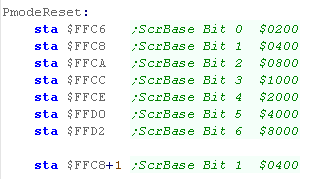
The example code here will reset the screen base to $0400
Writes to $FFC6-D2 set all the bits to 0... Then bit 1 is set with a write to $FFC9.


Dragon Memory Map

Address Dragon Purpose
$0000 Direct Page
$0100 System Vectors
$0200 Casette Buffer
$0300 Line Input Buffer
$0400 Text Screen
$0600 Memory Page 1 / Vars
$0C00 Screen Page 2 / Program
$1200 Graphics Page 3 / Basic
$1800 Normal Page 4 / Extra
$1E00 Memory Page 5 / Variables
$2400 Screen Page 6 / Program
$2A00 Graphics Page 7 / Basic
$3000 Extra Page 8 / Normal
$3600 Program / Var Storage & Stack (SP=$7F36)
$7F36 String Space
$8000 Basic Interpreter
$C000 Cartridge Memory
$FF00 PIA0 A Data direction Register / Peripheral Data Register
$FF01 PIA0 A Control Register
$FF02 PIA0 B Data direction Register / Peripheral Data Register
$FF03 PIO0 B Control Register
$FF20 PIA1 A Data direction Register / Peripheral Data Register
$FF21 PIA1 A Control Register
$FF22 PIA0 B Data direction Register / Peripheral Data Register
$FF23 PIA1 B Control Register
$FF60 Reserved
$FFC0 Clear V0
$FFC1 Set V0
$FFC2 Clear V1
$FFC3 Set V1
$FFC4 Clear V2
$FFC5 Set V2
$FFC6 Reset Screen Addr Bit 0
$FFC7 Set Screen Addr Bit 0
$FFC8 Reset Screen Addr Bit 1
$FFC9 Set Screen Addr Bit 1
$FFCA Reset Screen Addr Bit 2
$FFCB Set Screen Addr Bit 2
$FFCC Reset Screen Addr Bit 3
$FFCD Set Screen Addr Bit 3
$FFCE Reset Screen Addr Bit 4
$FFCF Set Screen Addr Bit 4
$FFD0 Reset Screen Addr Bit 5
$FFD1 Set Screen Addr Bit 5
$FFD2 Reset Screen Addr Bit 6
$FFD3 Set Screen Addr Bit 6
$FFE0 Reserved
$FFF2 SWi 3 Vector
$FFF4 SWI 2 Vector
$FFF6 FIRQ Vector
$FFF8 IRQ Vector
$FFFA SWI 1 Vector
$FFFC NMI Vector
$FFFE Reset Vector

Keyboard Matrix
PAx = bits read from $FF00
PBx = Write to $FF02 with byte containing zero at this point, eg PB0=%11111110


PB0 (W)
PB1 (W) PB2 (W) PB3 (W) PB4 (W) PB5 (W) PB6 (W) PB7 (W)
PA0 (R)
0 1 2 3 4 5 6 7
PA1 (R) 8 9 *
, - /
PA2 (R) @ A B C D E F G
PA3 (R) H I J K L M N 0
PA4 (R) P Q R S T U V W
PA5 (R) X Y Z Up Down Left Right Space
PA6 (R) ENT CLR BRK N/C N/C N/C N/C SHFT
PA7 (R) JoyTest JoyTest JoyTest JoyTest JoyTest JoyTest JoyTest JoyTest

PIA0 / PIA1 - Peripheral Interface Adapters

The PIA's select and send and receive data from the graphics chip, Keyboard, Joystick, Printer (RS232) and Sound hardware

The Data ports also double up as a 'Direction Select port' (Via bit 2 of the control port)... writing a 1 bit selects Direction IN... writing a 0 selects Direction OUT

$FF00 
Dir 
PIA0-A Data
Bit 7 I Joy compare (Compare to $FF20)
Bit 6 I Key row PA6 (select with $FF02)
Bit 5 I Key row PA5 (select with $FF02)
Bit 4 I Key row PA4 (select with $FF02)
Bit 3 I Key row PA3 (select with $FF02)
Bit 2 I Key row PA2 (select with $FF02)
Bit 1 I Key row PA1 (select with $FF02)
Bit 0 I Key row PA0 (select with $FF02)


$FF01
PIA0-A Control
Bit 7
IRQA1: HSYNC Flag
Bit 6
IRQA2: Unused
Bit 5
1 -> CA2 in CRA3 in bit follow mode
Bit 4
1 -> CA2 in CRA3 in bit follow mode
Bit 3
CA2: Select Device (Multiplexor LSB)
Bit 2
Dir/Data: 0=$FF00 Selects Direction 1=$FF00 Access Data
Bit 1
CA1 ctrl: 0=IRQ on Hi to Low... 1=IRQ on Low to Hi
Bit 0
CA1 IRQ: 0=off 1=on


$FF02 Dir PIA0-B Data
Bit 7 O Key Col PB7 / Printer P7
Bit 6 O Key Col PB6 / Printer P7
Bit 5 O Key Col PB5 / Printer P7
Bit 4 O Key Col PB4 / Printer P7
Bit 3 O Key Col PB3 / Printer P7
Bit 2 O Key Col PB2 / Printer P7
Bit 1 O Key Col PB1 / Printer P7
Bit 0 O Key Col PB0 / Printer P7


$FF03
PIA0-B Control
Bit 7
IRQB1: VSYNC Flag
Bit 6
IRQB2: Unused
Bit 5
1 -> CB2 in CRB3 in bit follow mode
Bit 4
1 -> CB2 in CRB3 in bit follow mode
Bit 3
CB2: Select Device (Multiplexor MSB)
Bit 2
Dir/Data: 0=$FF02 Selects Direction 1=$FF02 Access Data
Bit 1
CB1 ctrl: 0=IRQ on Hi to Low... 1=IRQ on Low to Hi
Bit 0
CB1 IRQ: 0=off 1=on


$FF20 Dir PIA1-A Data
Bit 7 O DAC Bit 5 (Joy Compare / Sound)
Bit 6 O DAC Bit 4 (Joy Compare / Sound)
Bit 5 O DAC Bit 3 (Joy Compare / Sound)
Bit 4 O DAC Bit 2 (Joy Compare / Sound)
Bit 3 O DAC Bit 1 (Joy Compare / Sound)
Bit 2 O DAC Bit 0 (Joy Compare / Sound)
Bit 1 O RS232 Out / Printer Strobe
Bit 0 I Casette In


$FF21
PIA1-A Control
Bit 7
IRQA1 Printer Ack Flag
Bit 6
IRQA2: Unused
Bit 5
CRA4 =1 -> CA2 in CRA3 bit follow mode
Bit 4
CRA4 =1 -> CA2 in CRA3 bit follow mode
Bit 3
CA2: Casette Motor (1=on)
Bit 2
Dir/Data: 0=$FF20 Selects Direction 1=$FF20 Access Data
Bit 1
CA1 ctrl: 0=IRQ on Hi to Low... 1=IRQ on Low to Hi
Bit 0
CA1 IRQ: 0=off 1=on


$FF22 Dir PIA1-B Data
Bit 7 O ScreenMode G/A
Bit 6 O ScreenMode GM2
Bit 5 O ScreenMode GM1
Bit 4 O ScreenMode GM0 / INT
Bit 3 O ScreenMode CSS
Bit 2 I Ram Size (1=16k 0=32/64k))
Bit 1 I Single bit sound
Bit 0 I Rs232 In / Printer Busy


$FF23
PIA1-B Control
Bit 7
IRQB1 Cartridge Interrupt
Bit 6
IRQB2: Unused
Bit 5
CRB4 =1 -> CB2 in CRB3 bit follow mode
Bit 4
CRB4 =1 -> CB2 in CRB3 bit follow mode
Bit 3
CB2: Sound Source Enable (1=on)
Bit 2
Dir/Data: 0=$FF22 Selects Direction 1=$FF22 Access Data
Bit 1
CB1 ctrl: 0=IRQ on Hi to Low... 1=IRQ on Low to Hi
Bit 0
CB1 IRQ: 0=off 1=on

Multiplexer Device selection

$FF23 Bit 3
$FF21 Bit 3
$FF03 Bit 3
$FF01 Bit 3
PIA1-CB2 PIA1-CA2 PIA0-CB2 PIA0-CA2
SoundSource 
Cassette Motor 
Multiplexer H 
Multiplexer
Purpose
0 ? 0 0 Write JJJJJJ-- to $FF20 .... Read ($FF00) Joystick R-X O-----LR O=1 means Over written value
0 ? 0 1 Write JJJJJJ-- to $FF20 .... Read ($FF00) Joystick R-Y O-----LR O=1 means Over written value
0 ? 1 0 Write JJJJJJ-- to $FF20 .... Read ($FF00) Joystick L-X O-----LR O=1 means Over written value
0 ? 1 1 Write JJJJJJ-- to $FF20 .... Read ($FF00) Joystick L-Y O-----LR O=1 means Over written value
1 ? 0 0 Write SSSSSS-- to $FF20 .... 6 Bit DAC
1 ? 0 1 Cassette
1 ? 1 0 Cartridge
1 ? 1 1 Unused

Basic Commands

Reserved word Token Dispatch address
FOR 80 8448
GO(TO/SUB) 81 85B9
REM 82 8616
' 83 8616
ELSE 84 8616
IF 85 8647
DATA 86 8613
PRINT 87 903D
ON(GOTO/SUB) 88 8675
INPUT 89 872B
END 8A 8532
NEXT 8B 8829
DIM 8C 8A8B
READ 8D 8777
LET 8E 86BC
RUN 8F 85A5
RESTORE 90 8514
RETURN 91 85F3
STOP 92 8539
POKE 93 8E9D
CONT 94 8560
LIST 95 8EAA
CLEAR 96 8571
NEW 97 8415
DEF 98 9C81
CLOAD 99 B6D5
CSAVE 9A B683
OPEN 9B B829
CLOSE 9C B64D
LLIST 9D 8EA4
SET 9E B9D3
RESET 9F BA04
CLS A0 BA60
MOTOR A1 B982
SOUND A2 BA9B
AUDIO A3 BADF
EXEC A4 B771
SKIPF A5 B81F
DELETE A6 9D61
EDIT A7 9965
TRON A8 9AD9
TROFF A9 9ADA
LINE AA A749
PCLS AB A8C0
PSET AC A6EF
PRESET AD A6F3
SCREEN AE A9FE
PCLEAR AF AA19
COLOR BO A8D4
CIRCLE B1 B238
PAINT B2 AC87
GET B3 AAF0
PUT B4 AAF3
DRAW B5 B051
PCOPY B6 AABE
PMODE B7 A9AF
PLAY B8 ADBD
DLOAD B9 A049
RENUM BA 9DFA

Interrupt Vectors
Address Vector (Address) Registers Auto-pushed onto stack
$FFF2 SWi 3 Vector ($0100) D,X,Y,U,DP,CC
$FFF4 SWI 2 Vector ($0103) D,X,Y,U,DP,CC
$FFF6 FIRQ Vector ($010F) CC
$FFF8 IRQ Vector ($010C) D,X,Y,U,DP,CC
$FFFA SWI 1 Vector ($0106) D,X,Y,U,DP,CC
$FFFC NMI Vector ($0109) D,X,Y,U,DP,CC
$FFFE RESET Vector ($B3B4) NA