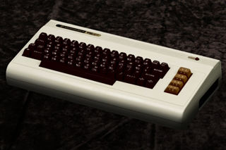
Due to it's memory limitations, we won't be using the Vic-20 as much as some other systems, but there's still plenty of impressive stuff this early machine can do!


|
 |
Useful Documents
ChibiAkumas Tutorials
Memory Map
| Address | Purpose |
| $0000-$01FF | ZeroPage/Stack etc |
| $0200-$03FF | OS memory |
| $0400-$0FFF | 3K RAM Upgrade |
| $1000-$1DFF | User Memory (screen memory with extra ram) |
| $1E00-$1FFF | Screen Memory |
| $2000-$7FFF | Rom area |
| $8000-$8FFF | Character Rom |
| $9000-$900F | VIC Registers |
| $9110-$911F | VIA
1 (Timer 1 causes NMI) |
| $9120-$912F | VIA
2 (Timer 1 causes IRQ) |
| $9400-$95FF | (Character colors with extra ram) |
| $9600-$97FF | Character Colors |
| $A000-$BFFF | Cartridge ROM |
| $C000-$DFFF | Basic ROM |
| $E000-$FFFF | Kernel ROM |

| Address | Suggested Value | Meaning |
| $9000 | $0C | horizontal centering |
| $9001 | $26 | vertical centering |
| $9002 | $96 ($16)* | set # of columns, bit 7 is part of screen address |
| $9003 | $AE | set # of rows |
| $9004 | $7A | TV raster beam line |
| $9005 | $FF ($CF)* | bits 0-3 start of character memory / bits 4-7 is rest of video address |
| $9006 | $57 | horizontal position of light pen |
| $9007 | $EA | vertical position of light pen |
| $9008 | $FF | Digitized value of paddle X |
| $9009 | $FF | Digitized value of paddle Y |
| $900A | $00 | Frequency for oscillator 1 (low) |
| $900B | $00 | Frequency for oscillator 2 (medium) |
| $900C | $00 | Frequency for oscillator 3 (high) |
| $900D | $00 | Frequency of noise source |
| $900E | $00 | bit 0-3 sets volume of all sound / bits 4-7 are auxiliary color information |
| $900F | $66+8 | Screen and border color register |
| 0 | 1 | 2 | 3 | 4 | 5 | 6 | 7 |
| Border | ||||||||
| Background | Black | White | Red | Cyan | Purple | Green | Blue | Yellow |
| Black | 08 | 09 | 0A | 0B | 0C | 0D | 0E | 0F |
| White | 18 | 19 | 1A | 1B | 1C | 1D | 1E | 1F |
| Red | 28 | 29 | 2A | 2B | 2C | 2D | 2E | 2F |
| Cyan | 38 | 39 | 3A | 3B | 3C | 3D | 3E | 3F |
| Purple | 48 | 49 | 4A | 4B | 4C | 4D | 4E | 4F |
| Green | 58 | 59 | 5A | 5B | 5C | 5D | 5E | 5F |
| Blue | 68 | 69 | 6A | 6B | 6C | 6D | 6E | 6F |
| Yellow | 78 | 79 | 7A | 7B | 7C | 7D | 7E | 7F |
| Orange | 88 | 89 | 8A | 8B | 8C | 8D | 8E | 8F |
| Light Orange | 98 | 99 | 9A | 9B | 9C | 9D | 9E | 9F |
| Pink | A8 | A9 | AA | AB | AC | AD | AE | AF |
| Light Cyan | B8 | B9 | BA | BB | BC | BD | BE | BF |
| Light Purple | C8 | C9 | CA | CB | CC | CD | CE | CF |
| Light Green | D8 | D9 | DA | DB | DC | DD | DE | DF |
| Light Blue | E8 | E9 | EA | EB | EC | ED | EE | EF |
| Light Yellow | F8 | F9 | FA | FB | FC | FD | FE | FF |
| The Vic-20 has no bitmap graphics! however it can use a
custom character set, so we can effectively fake 8x8 'tiles' using
this option the low nibble of $9005 defines the position of the characters, though some options are unusable, here are the options, and where in memory the characters will be read. the high nibble is used to define the video address, so should not be altered... it's default value is $F , but you can read it in, and OR in your new character source The best position for it is at $1C00... and example of how to do this is shown to the right. This will give you 128 definable characters between 0-127... the normal A-Z char map will start from character 128 |
lda $9005 and #$F0 ora #$0F sta $9005 ;Set character Ram Location ----LLLL |
| $9005 Low Nibble | value in bits | Type | Hex addr | Dec Addr |
| 0 | 0000 | ROM | $8000 | 32768 |
| 1 | 0001 | ROM | $8400 | 33792 |
| 2 | 0010 | ROM | $8800 | 34816 |
| 3 | 0011 | ROM | $8C00 | 35840 |
| 8 | 1000 | RAM | $0000 | 0 |
| 9 | 1001 | N/A | xxxx | xxxx |
| A | 1010 | N/A | xxxx | xxxx |
| B | 1011 | N/A | xxxx | xxxx |
| C | 1100 | RAM | $1000 | 4096 |
| D | 1101 | RAM | $1400 | 5120 |
| E | 1110 | RAM | $1800 | 6144 |
| F | 1111 | RAM | $1C00 | 7168 |
| Bits | Source | Address |
| 00 | Screen Color | $900F CCCC---- |
| 01 | Border Color | $900F ----CCCC |
| 10 | Character color | $9600 - $97FF |
| 11 | AuxColor | $900F CCCC---- |
Interrupt Vectors
The standard 6502 interrupt vectors from $FFFA+ are ROM, however these jump to vectors in low memory addresses. IRQ and BRK interrupts push A,X and Y onto the stack in that order.
Timer 1 on VIA 1 causes an NMI interrupt
Timer 1 on VIA 2 causes an IRQ interrupt
Note: It seems there is no VBLANK interrupt on the VIC20!
| From | To | Function
|
Registers Pushed |
| $0314
|
$0315 |
INT | A X Y |
| $0316 | $0317 | BRK | A X Y |
| $0318 | $0319 | NMI |
Sound
There are 3 sound channels for the 3 different frequencies, one for
random noise, and a volume setting...
As well as volume The top 4 bits of the $900E also handles color
| Address | Meaning | Bits | Details |
| $900A | Frequency for oscillator 1 (Bass) | OFFFFFFF | O=On F=Frequency |
| $900B | Frequency for oscillator 2 (medium) | OFFFFFFF | O=On F=Frequency |
| $900C | Frequency for oscillator 3 (high freq) | OFFFFFFF | O=On F=Frequency |
| $900D | Frequency of noise source | OFFFFFFF | O=On F=Frequency |
| $900E | Volume of all sound / Auxiliary color information | CCCCVVVV | V=Volume C=Aux color |
File Header
| If we're creating a PRG file which we're going to run on the VIC,
we need a 'basic header', this is effetively a 'launcher' for the program... our code immediately follows. |
* = $1001 ; BASIC program to boot the machine language code db $0b, $10, $0a, $00, $9e, $34, $31, $30, $39, $00, $00, $00 |
| If we want to create a ROM cartridge, we can do this with a simple header... however there is a problem... the screen will not be set up, so we'll get a black screen until we set up the screen properly. | * = $A000 dw ProgramStart dw ProgramStart db $41,$30,$C3,$C2,$CD ;ROM Header ProgramStart: |
VIAs
| Address | Meaning | Bits | Details |
| $9110 | VIA1: Port B output register | ||
| $9111 | VIA1: Port A output register | ||
| $9112 | VIA1: Data direction register B | DDDDDDDD | Direction 0=read 1=write |
| $9113 | VIA1: Data direction register A | DDDDDDDD | Direction 0=read 1=write |
| $9114 | VIA1: Timer 1
low byte |
LLLLLLLL | Set Timer (60 hz) (Timer1=NMI) |
| $9115 | VIA1: Timer 1 high byte & counter | HHHHHHHH | Set Timer (60 hz) |
| $9116 | VIA1: Timer 1 low byte | LLLLLLLL | |
| $9117 | VIA1: Timer 1 high byte | HHHHHHHH | |
| $9118 | VIA1: Timer 2 low byte | LLLLLLLL | |
| $9119 | VIA1: Timer 2 high byte | HHHHHHHH | |
| $911A | VIA1: Shift register | SSSSSSSS | |
| $911B | VIA1: Auxiliary control register | 1O2SSSPP | 1=T1 Control PB7 Out / O=One shot free run / 2=T2 control PB6 sense / S=Shift register control / P=PB PA Latch control |
| $911C | VIA1: Peripheral control register | BBBbAAAa | B=CB2 (Pup) control in/out / b=CB1 in casette #2 / A= CA2 graphics lowecase in out / a=CA1 in polarity .... 12=Graphic |
| $911D | VIA1: Interrupt flag register | ITtBBSAa | I=IRQ status / T=T1 interrupt / t=T2 interrupt / B=CB1 Casette / S=SR Interrupt / A=CA1 Interrupt / a=CA2 Interrupt ... Write 255 to clear |
| $911E | VIA1: Interrupt enable register | ETtBbSAa | E=Enable or disable following ints / T=T1 interrupt / t=T2 interrupt / B=CB1 interrupt / b=CB2 Interrupt / S=SR interrupt / A=CA1 Interrupt / a=CA2 interrupt |
| $911F | VIA1: Port A | R------- | Joystick Right |
| $9120 | VIA2: Port B output register | --FLDU-- | Joystick Fire,Up, Down, Left |
| $9121 | VIA2: Port A output register | ||
| $9122 | VIA2: Data direction register B | DDDDDDDD | Direction 0=read 1=write |
| $9123 | VIA2: Data direction register A | DDDDDDDD | Direction 0=read 1=write |
| $9124 | VIA2: Timer 1
low byte |
LLLLLLLL | Set Timer (60 hz) (Timer1=IRQ) |
| $9125 | VIA2: Timer 1 high byte & counter | HHHHHHHH | Set Timer (60 hz) |
| $9126 | VIA2: Timer 1 low byte | LLLLLLLL | |
| $9127 | VIA2: Timer 1 high byte | HHHHHHHH | |
| $9128 | VIA2: Timer 2 low byte | LLLLLLLL | |
| $9129 | VIA2: Timer 2 high byte | HHHHHHHH | |
| $912A | VIA2: Shift register | SSSSSSSS | |
| $912B | VIA2: Auxiliary control register | 1O2SSSPP | 1=T1 Control PB7 Out / O=One shot free run / 2=T2 control PB6 sense / S=Shift register control / P=PB PA Latch control |
| $912C | VIA2: Peripheral control register | BBBbAAAa | B=CB2 (Pup) control in/out / b=CB1 in casette #2 / A= CA2 graphics lowecase in out / a=CA1 in polarity .... 12=Graphic |
| $912D | VIA2: Interrupt flag register | ITtBBSAa | I=IRQ status / T=T1 interrupt / t=T2 interrupt / B=CB1 Casette / S=SR Interrupt / A=CA1 Interrupt / a=CA2 Interrupt ... Write 255 to clear |
| $912E | VIA2: Interrupt enable register | ETtBbSAa | E=Enable or disable following ints / T=T1 interrupt / t=T2 interrupt / B=CB1 interrupt / b=CB2 Interrupt / S=SR interrupt / A=CA1 Interrupt / a=CA2 interrupt |
| $912F | VIA2: Port A | AAAAAAAA |