The PC-Engine uses a super-charged
version of the 65c02... which itself is an improved version of the
6502 
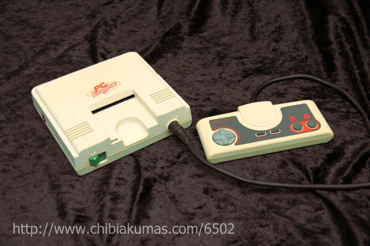
Known as the TurboGrafx-16, the PC-Engine is often mistaken for a 16 bit system because of its speed and graphical capability. There are various successors to the PC engine, but we'll only be covering the basic model. |
![]() |
||||||||||||||||||||||
|
ChibiAkumas Tutorials
Resources
PC Engine Docs - A
collection of PC Engine programming docs.
PC Engine GT Capacitor
list - For repairing the portable PC Engine
The PC engine uses an effective 21
bit memory map... 13 bits of the address specified, and 8 bits
from the MPR register The topmost 3 bits are mapped through a Memory Management unit which maps to Ram/Rom or hardware This is all a bit confusing, but it's really pretty easy This Memory management unit has 8 registers, each of which handles a range of $2000 of the memory map, and a bank from $00-$FF... $FF is the hardware I/O ... $F8 is the 8k of basic ram... $00 is the first page of your cartridge rom. To page in a bank, we need to specify it by 'bit position' (so bank 7 has bit 7 set... so 128) we load A with the bitmask for that MPR, then use the special command TAM (transfer A to MPR) eg: - lets load bank $F8 into MPR page 1 ($2000-$3FFF) lda #$F8 ;ram bank TAM #2 ;bit 2 for bank 2 (%00000010) NOTE: The ZeroPage is at $2000 , and the Stack is at $2100 ... this is unaffected by the MPR's.... this causes problems in VASM, where if we try to write STA $0000 ... the assembler will optimize it to STA $00 |
![]()
|
Segments
Bank | Purpose |
$FF | I/O |
$F9-$FB
|
SuperGrafx extra RAM (24k) |
$F8 | PC Engine RAM (8k) |
$F7 | Savegame RAM |
$00-$F6 | HuCard ROM |
Vectors
From (Logical) |
To (Logical) |
Purpose |
$FFF6 |
$FFF7 |
IRQ2 (External) / BRK |
$FFF8 |
$FFF9 |
IRQ1 (VDC / Vblank) |
$FFFA |
$FFFB |
Timer interrupt |
$FFFC |
$FFFD |
NMI |
$FFFE |
$FFFF |
- |
From (Physical) |
To (Physical) |
Purpose |
$00 1FFE |
$00 1FFF |
Reset |
The Reset vector should be at $5FFE in your rom, and should contain "DW $E000" to start your program
IO Ports
Address |
Purpose | Bits | Detail |
$0000 | GPU Reg Select (ST0) | NNNNNNNN | reg N |
$0002 | GPU Data L (ST1) | LLLLLLLL | Data L |
$0003 | GPU Data H (ST2) | HHHHHHHH | Data H |
$0400 | Palette: Reset | 00000000 | Write 0 to Reset |
$0402 | Palette: Palette Entry L | PPPPPPPP | Palette num (0-511) |
$0403 | Palette: Palette Entry H | -------P | Palette num (0-511) |
$0404 | Palette: New Color L | GGRRRBBB | Color |
$0405 | Palette: New Color H | -------G | Color |
$0800 | Channel Select | -----CCC | Channel Select |
$0801 | Main Amplitude Level | LLLLRRRR | L/R Volume |
$0802 | Frequency L | LLLLLLLL | Frequency botttom 8 bits |
$0803 | Frequency H | ----HHHH | Frequency top 4 bits |
$0804 | Channel On/Write | ED-VVVVV | Enable (play)/write data... Direct digitaldata� channel Volume |
$0805 | LR Volume | LLLLRRRR | L/R Volume |
$0806 | Waveform Data | ---WWWWW | Wave data (write 32 times) |
$0807 | Noise Enable | E--NNNNN | Enable noise� Noise freq (Chn 4/5 only) |
$0808 | LFO Freq | FFFFFFF | Noise freq (Chn 4/5 only) |
$0809 | LFO Control | T-----CC | lfo Trigger� Control |
$1000 | Joypad (Write) | ------CS | C=CLR S=SEL |
$1000 | Joypad (Read) | -C--DDDD | C=Country D=Joypad Data |
$1402 | Interrupt Disable | -----T12 | T=Timer interrupt request, 1= IRQ1 (Vblank), 2=IRQ2 (1=disabled) |
$1403 | Interrupt request | -----T12 | T=Timer interrupt request, 1= IRQ1 (Vblank),
2=IRQ2 (1=occurred) Write any values to clear Timer interrupt (Vblank is cleared by reading VDC Status at $0100) |
$1Ax0-$1Ax1 | Data Port 0/1 |
DDDDDDDD |
4 versions... Reg x (0-3) |
$1Ax2-$1Ax4 |
Base address (24 bit) |
$LLMMHH |
|
$1Ax5-$1Ax6 |
Offset Register |
$LLHH |
|
$1Ax7-$1Ax8 |
Increment Register |
$LLHH |
|
$1Ax9 | Control Register |
SOOIoiNA |
A=AutoInc N=iNdex offset + base i=increment is signed o=offset is
signed I=apply increment to base(1) or offset(0)? OO=offset mode(None/Port0/Port1/Port0+1) S=Dataport size(0=Byte 1=Word) |
$1AxA | Manual Register | Add offset to base | |
$1AE0-$1AE3 |
$LLMMHHUU | Work Register (32 bit) | |
$1AE4 |
Shift Register | ----SSSS | Signed Shift for work register |
$1AE5 |
Rotate Register | ----RRRR | Signed Rotate for work register |
$1AFE |
AC card version | DDDDDDDD | |
$1AFF |
AC ID | DDDDDDDD | $51=Present |
$1C00 | Timer Reload | -CCCCCCC | C=Counter |
$1C01 | Timer Control | -------S | Timer Start/Stop |
The PC-Engine Graphics
system
The PC Engine graphics hardware has 64k of ram... but it's
designed for 128k... it's controlled by a set of registers... we
have 3 hardware ports we use to control the hardware... these are
usually memory mapped to $0000 ... but we also have special commands
to quickly write fixed values to the graphics system We ALWAYS write data to the graphics system registers in HL byte pairs... Little Endian, so low byte first. To write data to the memory we set the address we want to write to with MAWR... but please note , we're only setting the last 16 of the 17 bits... for example, if we set MAWR to $3FFF (%11111111111111), the actual memory address will be %111111111111110 The effect is, that there are 2 bytes at VRAM $0000... and two bytes at VRAM $0001 ... and these bytes DO NOT OVERLAP!
Reading from Status register (eg LDA $0100) clears Vblank interrupt - otherwise it will 'refire'. |
Reg | Name | Meaning | Bits |
00 | MAWR | Memory Address Write | |
01 | MARR | Memory Address Read | |
02 | VRR/VWR | Vram Data Write / Vram Data Read | (AutoIncs
after Write) |
03 | Unused |
||
04 | Unused | ||
05 | CR | Control | - - - IW IW DR TE TE BB SB EX EX IE IE IE IE BB= Background on SB=Sprites on... IE bits 3-0 = Vblank / ScanLine match / SpriteOverflow / Collision |
06 | RCR | Scanning Line Detection | |
07 | BXR | BGX Scroll | |
08 | BYR | BGY Scroll | |
09 | MWR | Memory Access Width | - - - - - - - - CM SCR SCR SCR SM SM WV WV (SCR=Screen Width /Height %YXX) |
0A | HSR | Horizontal Sync | |
0B | HDR | Horizontal Display | |
0C | VPR | Vertical Sync | |
0D | BDW | Vertical Display | |
0E | BCR | Vertical Display End Position | |
0F | DCR | Block Transfer Control | |
10 | SOUR | Block Transfer Source Address | |
11 | DESR | Block Transfer Destination Address | |
12 | LENR | Block Transfer Length | |
13 | SATB | VRAM-SATB Block Transfer Source |
Memory in the VRAM is not entirely fixed in purpose, this means
you can have weird effects, like using the same memory area for your
Tilemaps - and tile definitions (Patterns)... this is totally
useless, as one will corrupt the other, but we have to understand it's possible to understand the memory... as stated before, each address has 2 bytes... A Pattern (tile definition) is 32 bytes in size (4 bitplanes, 8 lines)... and because each memory address in the VRAM map contains 2 bytes... the pattern will take up 16 memory addresses... this means tile 0 starts at $0000... and tile 1 is at $0010 NOW... the TileMap has to be at $0000 .. and it takes AT LEAST $0400 (it's minimum size is 32x32, and each definition takes 2 bytes)... so we can't use tiles 0-64 for ease, it's probably easiest to start your pattern definitions at no 256 (memory address $1000) |
|
F | E | D | C | B | A | 9 | 8 | 7 | 6 | 5 | 4 | 3 | 2 | 1 | 0 | |
- | - | - | - | - | - | - | G | G | G | R | R | R | B | B | B |
Port | Purpose | 7
|
6
|
5
|
4
|
3
|
2
|
1
|
0
|
$0400 | Write 0 to Reset | 0 | 0 | 0 | 0 | 0 | 0 | 0 | 0 |
$0402 | Palette Entry L | P | P | P | P | P | P | P | P |
$0403 | Palette Entry H | - | - | - | - | - | - | - | P |
$0404 | New Color L | G | G | R | R | R | B | B | B |
$0405 | New Color H | - | - | - | - | - | - | - | G |
Palette Entry | Purpose | ||||||||
0-255 | Background | ||||||||
256-511 | Sprites |
As with everything else on the PC engine Vram... each tile
definition takes one memory address, which contains 2 bytes... The top 4 bits pppp define a 16 color palette number from 0-15... The remaining 12 bits nnnn nnnnnnnn define the tile number - as stated, the first 64-256 probably can't be used because they overlap the tilemap... no's 2048-4095 CANNOT be used, as the memory these would use would be 64k-128k... and this memory is not installed in the PC Engine. |
ppppnnnn nnnnnnnn |
Byte 1 | Byte 2 | |
First 16 bytes | 00111100 01111111 01100011 01100011 01111111 01100011 01100011 00000000 |
00222200 02222222 02200022 02200022 02222222 02200022 02200022 00000000 |
Second 16 bytes | 00333300 03333333 03300033 03300033 03333333 03300033 03300033 00000000 |
00444400 04444444 04400044 04400044 04444444 04400044 04400044 00000000 |
For Example lets look at a sprite, where all pixels are color 0 or color 15!
|
|
Address | F | E | D | C | B | A | 9 | 8 | 7 | 6 | 5 | 4 | 3 | 2 | 1 | 0 | Notes | |
1 | - | - | - | - | - | - | Y | Y | Y | Y | Y | Y | Y | Y | Y | Y | Y=Ypos (64 is first visible line) | |
2 | - | - | - | - | - | - | X | X | X | X | X | X | X | X | X | X | X=Xpos (32 is first visible line) | |
3 | - | - | - | - | - | A | A | A | A | A | A | A | A | A | A | A | A=Address (Top 10 bits $trueaddress>>5 ) | |
4 | YF | - | YS | YS | XF | - | - | XS | F | - | - | - | P | P | P | P | YF=Yflip XF=Xflip YS=Ysize (16/32/64) XS=Xsize (16/32) F=Foreground (infront of tilemap) P=Palette (256+) |
Joypad | Select bit (Bit 0 $1000) |
7 | 6 | 5 | 4 | 3 |
2 |
1 | 0 |
1 | 1 | CD addon (1=yes) |
Country (0=jpn) |
- | - | Left | Down | Right | Up |
1 | 0 | CD addon (1=yes) |
Country (0=jpn) |
- | - | Run | Start | B | A |
2 | 1 | CD addon (1=yes) |
Country (0=jpn) |
- | - | Left | Down | Right | Up |
2 | 0 | CD addon (1=yes) |
Country (0=jpn) |
- | - | Run | Start | B | A |
The PC Engine
actually supports 5 joypads, but Joypads 3-5 work in exatly the
same way, we just need to keep reading in from the same port. |
![]() |
The PSG Sound generator
The PC Engine PSG has 6 wave based
sound channels... each one uses 32 wave samples, of 5 bits each. We have to snd some commands to $0804 to tell the PSG we're going to write data.. then send the data to $0806 We also need to set the volumes correctly! To the right is a working example which will play a sound wave. |
lda #0 sta $0800;Channel Select lda #255 ;Mixing sta $0801 lda #1 ;Tone L sta $0802 lda #10 ;Tone H sta $0803 lda #%00011111 ;Chanel Op - Set 'Data Write' sta $0804 lda #%01011111 ;Chanel Op - Set 'Reset Write Address' sta $0804 lda #255 sta $0805 ;LR Volume ldy #4 ChibiSoundMoreWaves: lda #%00011111 sta $0806 sta $0806 sta $0806 sta $0806 lda #%00000000 sta $0806 sta $0806 sta $0806 sta $0806 dey bne ChibiSoundMoreWaves lda #%10011111 ;Chanel Op - Set 'Play' sta $0804 rts |
The PSG is controlled by 10 registers... first a channel should be selected with Register 0... Channels are numbered 0-5 (written 1-6 in the manuals)
Reg | Address | Meaning | Channels | 7 | 6 | 5 | 4 | 3 | 2 | 1 | 0 | Bit Meaning |
0 | $0800 | Channel Select | All | - | - | - | - | - | C | C | C | Channel Select |
1 | $0801 | Main Amplitude Level | All | L | L | L | L | R | R | R | R | L/R Volume |
2 | $0802 | Frequency L | 0-5 | L | L | L | L | L | L | L | L | Frequency botttom 8 bits |
3 | $0803 | Frequency H | 0-5 | - | - | - | - | H | H | H | H | Frequency top 4 bits |
4 | $0804 | Channel On/Write | 0-5 | E | D | - | V | V | V | V | V | Enable (play)/write data... Direct digitaldata� channel Volume |
5 | $0805 | LR Volume | 0-5 | L | L | L | L | R | R | R | R | L/R Volume |
6 | $0806 | Waveform Data | 0-5 | - | - | - | W | W | W | W | W | Wave data (write 32 times) |
7 | $0807 | Noise Enable | 0-5 | E | - | - | N | N | N | N | N | Enable noise� Noise freq (Chn 4/5 only) |
8 | $0808 | LFO Freq | All | F | F | F | F | F | F | F | F | lfo Frequency |
9 | $0809 | LFO Control | All | T | - | - | - | - | - | C | C | lfo Trigger� Control |