
Z80 Assembly programming for the Amstrad CPC
| The CPC was a popular home computer
in the 1980s and early 90s, and was used heavily by families for
games and very simple computing home computing tasks like word
processing. Like many systems of the era, it came with a built in Basic interpreter, so was the introduction to programming for many 80's era kids! While slower in some ways than the C64, it had far superior graphical capabilities to the ZX Spectrum, and usually beats the MSX for graphical speed because of it's smaller screen footprint (16k on the CPC to 24k on the MSX) and its CRTC graphics chip is favored by the modern clever demo authors. The CRTC chip also allows the screen to be resized, it can be 'shrunk' to a spectrum size screen of 256x192, or extended to an 'overscan' size of 384x272, where there are effectively no 'borders' around the screen and the image fills the CRTC area The budget tape-based 464 machine had 64k of memory, however the more expensive disk based system, known as the 6128 - has 128k and a 3" disk drive, and after market upgrades can give the machine up to 576k of memory! It should also be noted that the 464 can also be upgraded with a disk drive and extra memory. There were two major generations of the CPC, the regular 'original version, and the Plus versions released in the 90s, which has has hardware sprites, enhanced color. These Plus models were intended to compete with games consoles of the era, like the NES and SMS, however these were far too late, and did not offer enough extra performance to compete with the games consoles and 16 bit computers, so died out relatively quickly. |
 |
|||||||||||||||||||||||||||||||||
|
ChibiAkumas Tutorials:

Useful Documents!
CPC464_Firmware_1984_AMSOFT - The official breakdown of the rom
functions
CRTC - Details of the
amstrad CPC CRTC hardware
Amstrad
Firmware guide - Pdf documenting the CPC firmware calls
CPC
Firmware
Guide - Detailed info on how to use the CPC hardware and firmware
Basic Manual
- You'll want to know at least enough basic to do calls and operate the
computer
AY sound chip PDF - Manual for the sound chip (Warning! Reg-numbers
are in OCTAL! R10 is actually Reg 8)
CPC
Firmware disassembly - If you can't find what you need elsewhere,
you can always look at the source code!
Memory Map
Here is an overview of the Amstrad CPC Memory Map.Note, &0000-&3FFF can be paged in to basic ROM, &C000-&FFFF can be paged in to DISK ROM, and that the screen can be relocated anywhere in the 64k address space if required.
| &0000 |
&0000:LowJumpblock
|
&0100:Basic |
| &1000 | ||
| &2000 | ||
| &3000 |
|
|
| &4000 | &4000-&7FFF: 128k+ Bank switching | |
| &5000 | ||
| &6000 | ||
| &7000 | ||
| &8000 | ||
| &9000 | ||
| &A000 | &A600:AMSDOS | |
| &B000 | &B900:UpperJmpBlk
|
&BF00:Stack |
| &C000 | Screen | |
| &D000 | Screen | |
| &E000 | Screen | |
| &F000 | Screen |
OUT/IN Port Numbers
Here is an overview of the Amstrad CPC Memory Map.
Note, &0000-&3FFF can be paged in to basic ROM,
&C000-&FFFF can be paged in to DISK ROM, and that the screen can
be relocated anywhere in the 64k address space if required.
| BC | Purpose |
| &7Fxx | Gate Array & RAM Management (Rom / Ram Palette) |
| &BCrr | CRTC - Register Select rr |
| &BDdd | CRTC - Register Write dd |
| &BExx | CRTC - Model dependent |
| &BFxx | CRTC - Model dependent |
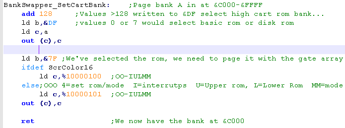
| &DFxx | ROM select (BASIC / DISK & CPC+ Cart) |
| &EFxx | Printer port |
| &F4xx | Port A Data (R/W) In/Out PSG (Sound/Keyboard/Joystick) |
| &F5xx | Port B Data (R/W) In Vsync/Jumpers/PrinterBusy/CasIn/Exp |
| &F6xx | Port C Data (R/W) Out KeybRow/CasOut/PSG |
| &F7xx | Control (W) Out Control |
| &F8xx | Expansion Peripherals |
| &F9xx | Expansion Peripherals |
| &FA7E | Floppy Motor Off (may get stuck on after save) |
| &FBxx | Expansion Peripherals |
Gate Array:
The Gate array is at port &7Fxx.. It can be accessed by loading B with &7F and performing 'OUT (C),C' or 'OUT (C),A'
It has multiple purposes depending on the top two bits passed in the C/A byte (xx)| 7 | 6 | 5 | 4 | 3 | 2 | 1 | 0 | Name | Bit meanings |
| 0 | 0 | - | B | P | P | P | P | Pen Selection | B=Border P=Pen (0-3 / 0-15) |
| 0 | 1 | - | C | C | C | C | C | Palette color selection | C= Color number (0-26) |
| 1 | 0 | - | I | H | L | M | M | Rom / Mode | I=
Interrupt mode
H=High rom bank enable (0=on 1=off.. &C000-&FFFF range... Disk / CPC+ Bank 0-31) L=Low rom bank enable (0=on 1=off... &0000-&3FFF range... Basic / CPC+ Bank 0-7) M=screen mode |
| 1 | 1 | B | B | B | R | R | R | Ram Bank | R = Ram config B= Bank number (0=128k 1+2=256k etc) |
Ram Banking
There are 7 options for ram banking on the 128k CPC:
| CPC | C0 | C1 | C2 | C3 | C4 | C5 | C6 | C7 |
| 0000-3FFF
|
RAM_0
|
RAM_0
|
RAM_4
|
RAM_0
|
RAM_0
|
RAM_0
|
RAM_0
|
RAM_0
|
| 4000-7FFF | RAM_1 | RAM_1 | RAM_5 | RAM_3 | RAM_4 | RAM_5 | RAM_6 | RAM_7 |
| 8000-BFFF | RAM_2 | RAM_2 | RAM_6 | RAM_2 | RAM_2 | RAM_2 | RAM_2 | RAM_2 |
| C000-FFFF | RAM_3 | RAM_7 | RAM_7 | RAM_7 | RAM_3 | RAM_3 | RAM_3 | RAM_3 |
Extra banks continue in the same way:
| 64K | 128K | 192K | ||||||||||||||
| C0 | C1 | C2 | C3 | C4 | C5 | C6 | C7 | C8 | C9* | CA | CB* | CC | CD | CE | CF | |
| RAM_0 | RAM_0 | RAM_4 | RAM_0 | RAM_0 | RAM_0 | RAM_0 | RAM_0 | RAM_0 | RAM_0* | RAM_8 | RAM_0* | RAM_0 | RAM_0 | RAM_0 | RAM_0 | |
| RAM_1 | RAM_1 | RAM_5 | RAM_3 | RAM_4 | RAM_5 | RAM_6 | RAM_7 | RAM_1 | RAM_1* | RAM_9 | RAM_3* | RAM_8 | RAM_9 | RAM_10 | RAM_11 | |
| RAM_2 | RAM_2 | RAM_6 | RAM_2 | RAM_2 | RAM_2 | RAM_2 | RAM_2 | RAM_2 | RAM_2* | RAM_10 | RAM_2* | RAM_2 | RAM_2 | RAM_2 | RAM_2 | |
| RAM_3 | RAM_7 | RAM_7 | RAM_7 | RAM_3 | RAM_3 | RAM_3 | RAM_3 | RAM_3 | RAM_11 | RAM_11 | RAM_11 | RAM_3 | RAM_3 | RAM_3 | RAM_3 | |
... And so on!
* This bank mode may not work on all hardware
The CRTC registers are selected with &BCxx (where xx is the register number)... and set with &BDxx (where xx is the new value| High Byte Value | F | E | D | C | B | A | 9 | 8 | Name |
| &BC | 1 | 0 | 1 | 1 | 1 | 1 | 0 | 0 | Register Select |
| &BD | 1 | 0 | 1 | 1 | 1 | 1 | 0 | 1 | Register Write |
CRTC registers will configure the Logical screen we draw on, and the physical screen shown by the Analog monitor...
You'll want to leave many of the settings alone, as they'll just result in a corrupt screen you can't view!
| Reg Num | Name | Range | Bits | Default
Value |
Speccy 256x192 |
Overscaln 384x272(26k) |
Details |
| &00 | Horizontal Total | 0-255 | DDDDDDDD | 63 | 63 | 63 | Physical width of screen � Leave alone! |
| &01 | Horizontal Displayed | 0-255 | DDDDDDDD | 40 | 32 | 48 | Logical width in Chars (8 pixels in mode 1) |
| &02 | Horizontal Sync Position | 0-255 | DDDDDDDD | 46 | 42 | 51 | Logical Xpos |
| &03 | Horizontal and Vertical Sync Widths | 0-15,0-15 | VVVVHHHH | 142 | 134 | 142 | Physical width of screen � Leave alone! |
| &04 | Vertical Total | 0-127 | -DDDDDDD | 38 | 38 | 38 | Physical height of screen � Leave alone! |
| &05 | Vertical Total Adjust | 0-31 | ---DDDDD | 0 | 0 | 0 | Scanline Offset |
| &06 | Vertical Displayed | 0-127 | -DDDDDDD | 25 | 24 | 34 | Logical Height in Chars (8 Pixels) |
| &07 | Vertical Sync position | 0-127 | -DDDDDDD | 30 | 31 | 35 | Logical Ypos of screen |
| &08 | Interlace and Skew | 0-3 | ------DD | 0 | 0 | 0 | 0/2=off 1/3=on � Leave alone! |
| &09 | Maximum Raster Address | 0-31 | ---DDDDD | 7 | 7 | 7 | Max Raster Address � Leave alone! |
| &0A | Cursor Start Raster | 0-127 | -DDDDDDD | 0 | 0 | 0 | |
| &0B | Cursor End Raster | 0-31 | ---DDDDD | 0 | 0 | 0 | |
| &0C | Display Start Address (H) | 0-63 | xxPPSSOO | 00 / 16 /
32 / 48 |
00 / 16 /
32 / 48 |
12+1 / 28 / 44+1 / 60 |
PP=Screen
Page (11=C000) S=Size(11=32k else 16k) O=Offset |
| &0D | Display Start Address (L) | 0-255 | OOOOOOOO | 0 | 0 | 0 | O=Offset |
| &0E | Cursor Address (H) | 0-63 | c--DDDDDD | 0 | 0 | 0 | |
| &0F | Cursor Address (L) | 0-255 | DDDDDDDD | 0 | 0 | 0 | |
| &10 | Light Pen Address (H) | 0-63 | --DDDDDD | 0 | 0 | 0 | Read Only |
| &11 | Light Pen Address (L) | 0-255 | DDDDDDDD | 0 | 0 | 0 | Read Only |
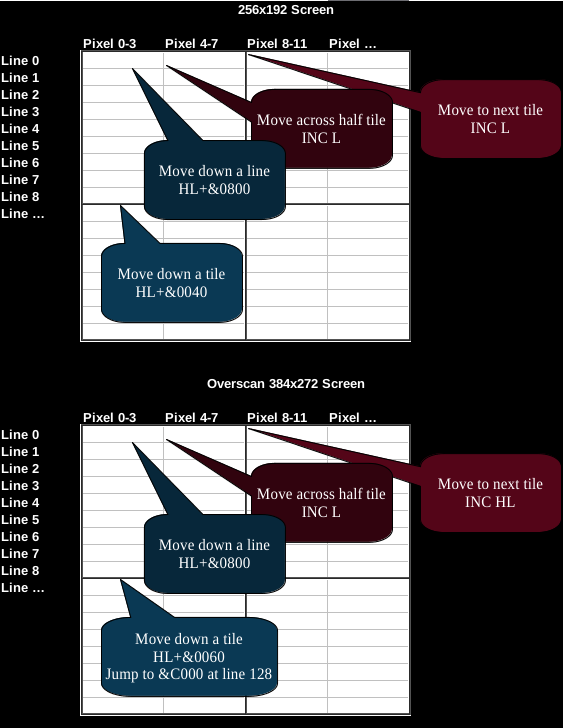
Here is a pictorial representation of the screen registers function:
CPC Palette
Each color has a firmware (basic) number and a hardware number (used with OUT)
Both are shown below in the format Firmware (0-26) - Hardware (40h-5Fh)
| 0 - 54h |
1 - 44h (or 50h) |
2 - 55h |
|
9 - 56h | 10 - 46h | 11 -
57h |
|
18 - 52h
|
19 - 42h
(or 51h) |
20 - 53h
|
| 3 - 5Ch | 4 - 58h | 5 - 5Dh | 12 - 5Eh
|
13 - 40h
(or 41h) |
14 - 5Fh | 21 - 5Ah | 22 - 59h | 23 - 5Bh | ||
| 6 - 4Ch | 7 - 45h (or 48h) |
8 - 4Dh | 15 - 4Eh | 16 47h | 17 - 4Fh | 24 - 4Ah | 25 -
43h (or 49h) |
26 - 4Bh |
Screen bit layout
The pixel bits are in different orders, depending on screen mode.
In the chart below: Numbers are the bit number, A-Z are the pixels
contained in the byte.
| Mode 2 Bits/Pixels |
A |
B |
C |
D |
E |
F |
G |
H |
| Mode 1 Bits/Pixels | A0 | B0 | C0 | D0 | A1 | B1 | C1 | D1 |
| Mode 0 Bits/Pixels | A0 | B0 | A2 | B2 | A1 | B1 | A3 | B3 |
Screen Memory
Not all 16K of the screen is used... The screen memory layout is split into strips of character blocks as shown below:
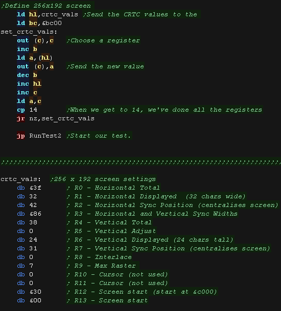
256x192 'speccy screen'
| The CPC's 320x200 screen is big, but most other systems used only
256x192, so this is often used by games as it makes things easier to
port. It also means the VRAM movement commands can only update the L part of the HL address, which increases speed a little too. We send a sequence of values to the CRTC chip to set up the screen layout. The 256x192 screen is 12k, but the CPC 'spreads' it over 16k, leaving some 512 byte blocks spare... we'll can use some of these for our work data! Free areas: &C600-&C7FF ;&200 *8 = &1000 free &CE00-&CFFF &D600-&D7FF &DE00-&DFFF &E600-&E7FF &EE00-&EFFF &F600-&F7FF &FE00-&FFFF |
 |
| The lines of the screen are split into two 'halves', these fill
the two 16k banks at &8000-&BFFF and &C000-&FFFF Lines 0-127 start at memory address base &8200 Lines 128-271 start at memory address base &C000 The formulas we need to use to move around memory are a bit more complex for Overscan which will make 'half tile' moves almost impossible, at least implausible for a example of this scope. With a 256 pixel, 64 byte wide screen we only needed to update L as we moved across the screen. But now, because our screen is 96 bytes wide, we will need to update H and L, at least when we move a full tile, the odd (mid tile) moves we can still just update L Moving down a line is the same as before, we add &0800 to HL, but moving over the 8 line boundary (down a tile) is more complex, as we have to cope with the 'jump' between the two banks (over address &B7FF we have to jump to &C000) |
 |
||
| A 384x272 @ 4 color screen should be about 25k, but it actually
covers 31k (&8200-&FEC0) The reason for this 'Discrepancy' is that there are gaps which are not used by the pixel data, which we can use for our work data - which may be important when half our 64k ram is used by the screen!!! Because the second bank has more screen lines (144), the &C000-&FFFF area has smaller unused areas. |
|
| We need to use an alternative set of CRTC settings to define our larger screen, and strange memory layout! | 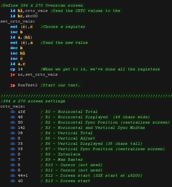 |
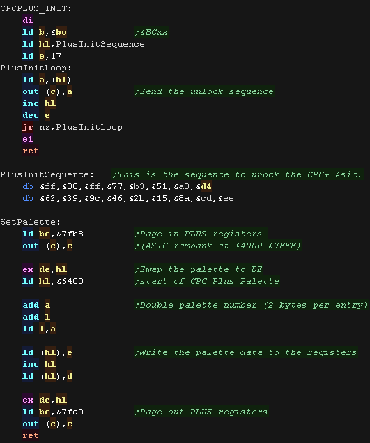
Turning on CPC+ features, and setting the Palette
| The CPC+ has a special bank of memory (Asic
registers) - These contain the palette and other CPC+ feature at the
memory address &4000-7FFF There is a special sequence to unock the CPC+ Asic we OUT it to &BC Once we've done this we can page in the ASIC with an OUT to &7FB8, we can page it out again with an OUT to &7FA0 CPC+ Colors are defined by 2 bytes from address &6400+ in the ASIC registers (CPC+ special ram)
NOTE: When using the ASIC memory, We should make sure that we paged out any extended 128k banks from the &4000-&7FFFF range, as it can cause problems using the plus registers while also paging memory in from 128k ram upgrades. Mode C1/C3 are OK to use as they page in at &C000. Of course you can use the extra memory during 'normal times' when the CPC+ ASIC memory is not in use Each color definition is 2 bytes, and there are definitions for the main 16 colors, the border, and CPC+ Hardware Sprites
We send two bytes in the format &-GRB ... where the - nibble is unused, G is Green, R is Red and B is blue |
 |
CPC+ Hardware sprites
The Amstrad CPC has 16 hardware sprites... each is 16x16
CPC+ sprites have a separate 16 colors to the normal palette, also they are always 16 color, even in mode 1!CPC+ Sprite colors (-GRB) are defined by the palette in memory range &6422-&643F
| Sprite Number | DataAddr (256bytes) | Xpos (2bytes) | Ypos (2bytes) | Resolution (1byte) |
| 1 | &4000 | &6000 | &6002 | &6004 |
| 2 | &4100 | &6008 | &600A | &600C |
| 3 | &4200 | &6010 | &6012 | &6014 |
| 4 | &4300 | &6018 | &601A | &601C |
| 5 | &4400 | &6020 | &6022 | &6024 |
| 6 | &4500 | &6028 | &602A | &602C |
| 7 | &4600 | &6030 | &6032 | &6034 |
| 8 | &4700 | &6038 | &603A | &603C |
| 9 | &4800 | &6040 | &6042 | &6044 |
| 10 | &4900 | &6048 | &604A | &604C |
| 11 | &4A00 | &6050 | &6052 | &6054 |
| 12 | &4B00 | &6058 | &605A | &605C |
| 13 | &4C00 | &6060 | &6062 | &6064 |
| 14 | &4D00 | &6068 | &606A | &606C |
| 15 | &4E00 | &6070 | &6072 | &6074 |
| 16 | &4F00 | &6078 | &607A | &607C |
The Amstrad CPC has 16 hardware sprites. Each is 16x16 CPC+ sprites have a separate 16 colors to the normal palette, also they are always 16 color, even in mode 1!
CPC+ Sprite colors (-GRB) are defined by the palette in memory range &6422-&643F
DataAddr is the sprite pattern data, note only the bottom nibble (4 bits) of each byte are used (%----CCCC), so a 16x16 sprite patternis 256 bytes
Xpos is 2 bytes, in little endian format. Screen co-ordinates are based on mode 2 - so xpos should be between -64 to +639 (0 is leftmost visible pixel)
Ypos is 2 bytes, in little endian format. Ypos should be between -64 to +200 (0 is topmost visible pixel)
| Resolution |
Result |
| %0000 (&0) |
Sprite Off |
| %0101 (&3) | Mode 2 scale |
| %1001 (&9) |
Mode 1 scale |
| %1101 (&D) | Mode 0 scale |
| %1110 (&E) |
2x Mode1 scale |
| %1111 (&F) | Vertically Stretched |
ASIC RAM and Cartridge ROM on the CPC+:
|
Asic Ram, when enabled appears at
&4000-&7FFF, but we also have cartridge ROM
On a CPC+ the Cartrige ROM has 32 banks... numbered 0-31... Banks 0-7 are intended to act as system ROM, appearing between &0000-&3FFF... however ANY bank (0-31) can be paged in at &C000-&FFFF - the same area as screen memory! Even better, if we WRITE to this area - it will be written to the screen RAM through the rom, so we don't need to page out the ROM to write data to the screen! Setting a rom bank is easy, we write the ROM we want to port &DF... values 0-7 will set the Low rom area number... setting the High rom area is done by adding 128 to the rom we want, and OUTing it to &DF Once we've selected it we still need to enable the rom, and we do this by writing to Bit 3 of the Gate array! |
 |
| To detect a CPC
Plus, we send the PLUS sequence, and turn on the ASIC ram.. .if
nothing happened we don't have a CPC+... we can use this fact to
detect a CPC! |
 |
 |
While you can write to
ASIC ram just like normal memory, don't rely on being able to read
from it! The development of ChibiAkumas ran into a problem, because reading the CPCPlus interrupt line from the ASIC worked on emulators... but not real hardware! It's probably best to assume you can't read back any writable ASIC values! |
Detecting the CPC+ and RAM:
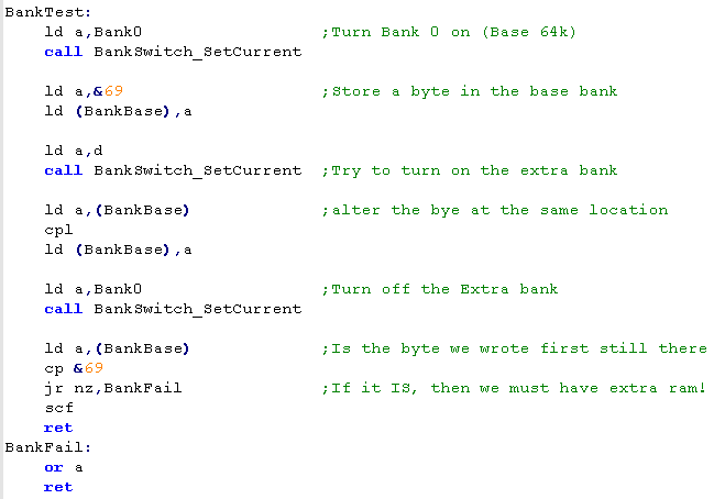
| So to detect RAM and the PLUS ASIC,
we need to set a byte in our normal memory, turn on the feature (RAM
or ASIC)... and WRITE to the same location - then turn off the
feature... If the byte we wrote isn't there, then we know the feature does not exist! In this code we'll use &69 as a byte that we'll write to the test location, and CPL to flip the bits of the location when we test. |
 |
| While each system is different We're
going to use a fairly generic detection function... It will return a value in DE... where D is the hardware type and E is the memory available On the CPC, D will be 1 if the machine is a PLUS, and E will be 0,1 or 2 depending if the machine is 64k,128k or 256k It's intended this function is executed at the start of your program, so the game can switch to different functions (or even load a different version of the game) depending on the platform. |
Keyboard Matrix
| Bit | ||||||||
| 7 | 6 | 5 | 4 | 3 | 2 | 1 | 0 | |
| &40 | F. | F-ENT | F3 | F6 | F9 | Cur-D | Cur-R | Cur-U |
| &41 | F0 | F2 | F1 | F5 | F8 | F7 | CPY | Cur-L |
| &42 | c | \ | SHIFT | 4 | ] | RET | [ | c |
| &43 | . | / | : | ; | P | @ | - | ^ |
| &44 | , | M | K | L | I | O | 9 | 0 |
| &45 | Space | N | J | H | Y | U | 7 | 8 |
| &46 | V | B J2-F3 | F J2-F2 | G J2-F1 | T J2-R | R J2-L | 5 J2-D | 6 J2-U |
| &47 | X | C | D | S | W | E | 3 | 4 |
| &48 | Z | CAPS | A | TAB | Q | ESC | 2 | 1 |
| &49 | DEL | J1-F3 | J1-F2 | J1-F1 | J1-R | J1-L | J1-D | J1-U |
AY Sound Chip:
| Register | Meaning | Bit Meaning | Details |
| 0 | Tone Pitch L - Channel A (Left) | LLLLLLLL | Lower value = Higher pitch |
| 1 | Tone Pitch H - Channel A (Left) | ----HHHH | Lower value = Higher pitch |
| 2 | Tone Pitch L - Channel B (Center) | LLLLLLLL | Lower value = Higher pitch |
| 3 | Tone Pitch H - Channel B (Center) | ----HHHH | Lower value = Higher pitch |
| 4 | Tone Pitch L - Channel C (Right) | LLLLLLLL | Lower value = Higher pitch |
| 5 | Tone Pitch H - Channel C (Right) | ----HHHH | Lower value = Higher pitch |
| 6 | Noise Generator | ---NNNNN | Higher value = Faster noise |
| 7 | Mixer | --NNNTTT | N=Noise T=Tone (Channel --CBACBA 1=mute 0=normal) |
| 8 | Amplitude - Channel A (Left) | ---EVVVV | E=Envelope (1=Enabled) VVVV=Volume |
| 9 | Amplitude - Channel B (Center) | ---EVVVV | E=Envelope (1=Enabled) VVVV=Volume |
| 10 | Amplitude - Channel C (Right) | ---EVVVV | E=Envelope (1=Enabled) VVVV=Volume |
| 11 | Envelope L (Volume over time) | LLLLLLLL | Lower value=Faster Envelope |
| 12 | Envelope H (Volume over time) | HHHHHHHH | Lower value=Faster Envelope |
| 13 | Envelope Selection | ----EEEE | Envelope number (See PDF) |
| 14 |
IO Port A | DDDDDDDD | Keyboard & Joystick |
| 15 |
IO Port B | DDDDDDDD | Not present on the AY-3-8912 |
Firmware Call List
| Low Area | High Jumpblock | Disk Rom |
| &0000 RESET ENTRY (RST0) &0008 LOW JUMP (RST1) &000B KL LOW PCHL (Jump to HL) &000E PCBC INSTRUCTION (Jump to BC) &0010 SIDE CALL (RST2) &0013 KL SIDE PCHL (Jump to HL in rom) &0016 PCDE INSTRUCTION (Jump to DE) &0018 FAR CALL (RST3) (Jump to inline 3 byte addr + Rom num) &001B KL FAR PCHL (Jump to HL in Rom C) &001E PCHL INSTRUCTION (Jump to HL) &0020 RAM LAM (Load A from HL in Ram) &0023 KL FAR CALL (Jump to inline 3 byte addr + Rom num pointed to by HL) &0028 FIRM JUMP (RST5) (Jump to inline 2 byte addr) &0030 USER RESTART (RST6) (spare) &0038 INTERRUPT ENTRY (RST7) (IM1 - occurs 6x per frame) &003B EXT INTERRUPT |
&B900 KL U ROM ENABLE &B903 KL U ROM DISABLE &B906 KL L ROM ENABLE &B909 KL L ROM DISABLE &B90C KL ROM RESTORE &B90F KL ROM SELECT &B912 KL CURR SELECTION &B915 KL PROBE ROM &B918 KL ROM DESELECT &B91B KL LDIR &B91E KL LDDR &B921 KL POLL SYNCHRONOUS &B92A KL SCAN NEEDED &BB00 KM INITIALISE &BB03 KM RESET &BB06 KM WAIT CHAR &BB09 KM READ CHAR &BB0C KM CHAR RETURN &BB0F KM SET EXPAND &BB12 KM GET EXPAND &BB15 KM EXP BUFFER &BB18 KM WAIT KEY &BB1B KM READ KEY &BB1E KM TEST KEY &BB21 KM GET STATE &BB27 KM SET TRANSLATE &BB2A KM GET TRANSLATE &BB2D KM SET SHIFT &BB30 KM GET SHIFT &BB33 KM SET CONTROL &BB36 KM GET CONTROL &BB39 KM SET REPEAT &BB3C KM GET REPEAT &BB3F KM SET DELAY &BB42 KM GET DELAY &BB45 KM ARM BREAK &BB48 KM DISARM BREAK &BB4B KM BREAK EVENT &BB4E TXT INITIALISE &BB51 TXT RESET &BB54 TXT VDU ENABLE &BB57 TXT VDU DISABLE &BB5A TXT OUTPUT &BB5D TXT WR CHAR &BB60 TXT RD CHAR &BB63 TXT SET GRAPHIC &BB66 TXT WIN ENABLE &BB69 TXT GET WINDOW &BB6C TXT CLEAR WINDOW &BB6F TXT SET COLUMN &BB72 TXT SET ROW &BB75 TXT SET CURSOR &BB78 TXT GET CURSOR &BB7B TXT CUR ENABLE &BB7E TXT CUR DISABLE &BB81 TXT CUR ON &BB84 TXT CUR OFF &BB87 TXT VALIDATE &BB8A TXT PLACE CURSOR &BB8D TXT REMOVE CURSOR &BB90 TXT SET PEN &BB93 TXT GET PEN &BB96 TXT SET PAPER &BB99 TXT GET PAPER &BB9C TXT INVERSE &BB9F TXT SET BACK &BBA2 TXT GET BACK &BBA5 TXT GET MATRIX &BBA8 TXT SET MATRIX &BBAB TXT SET M TABLE &BBAE TXT GET M TABLE &BBB1 TXT GET CONTROLS &BBB4 TXT STR SELECT &BBB7 TXT SWAP STREAMS &BBBA GRA INITIALISE &BBBD GRA RESET &BBC0 GRA MOVE ABSOLUTE &BBC3 GRA MOVE RELATIVE &BBC6 GRA ASK CURSOR &BBC9 GRA SET ORIGIN &BBCC GRA GET ORIGIN &BBCF GRA WIN WIDTH &BBD2 GRA WIN HEIGHT &BBD5 GRA GET W WIDTH &BBD8 GRA GET W HEIGHT &BBDB GRA CLEAR WINDOW &BBDE GRA SET PEN &BBE1 GRA GET PEN &BBE4 GRA SET PAPER &BBE7 GRA GET PAPER &BBEA GRA PLOT ABSOLUTE &BBED GRA PLOT RELATIVE &BBF0 GRA TEST ABSOLUTE &BBF3 GRA TEST RELATIVE &BBF6 GRA LlNE ABSOLUTE &BBF9 GRA LINE RELATIVE &BBFC GRA WR CHAR &BBFF SCR INITIALISE &BC02 SCR RESET &BC05 SCR SET OFFSET &BC08 SCR SET BASE &BC0B SCR GET LOCATION &BC0E SCR SET MODE &BC11 SCR GET MODE &BC14 SCR CLEAR &BC17 SCR CHAR LIMITS &BC1A SCR CHAR POSITION &BC1D SCR DOT POSITION &BC20 SCR NEXT BYTE &BC23 SCR PREV BYTE &BC26 SCR NEXT LINE &BC29 SCR PREV LINE &BC2C SCR INK ENCODE &BC2F SCR INK DECODE &BC32 SCR SET INK &BC35 SCR GET INK &BC38 SCR SET BORDER &BC3B SCR GET BORDER &BC3E SCR SET FLASHING &BC41 SCR GET FLASHING &BC44 SCR FILL BOX &BC17 SCR FLOOD BOX &BC4A SCR CHAR INVERT &BC4D SCR HW ROLL &BCS0 SCR SW ROLL &BC53 SCR UNPACK &BC56 SCR REPACK &BC59 SCR ACCESS &BC5C SCR PIXELS &BC5F SCR HORIZONTAL &BC62 SCR VERTICAL &BC65 CAS INITIALISE &BC68 CAS SET SPEED &BC6B CAS NOISY &BC6E CAS START MOTOR &BC71 CAS STOP MOTOR &BC74 CAS RESTORE MOTOR &BC77 *CAS IN OPEN &BC7A *CAS IN CLOSE &BC7D *CAS IN ABANDON &BC80 *CAS IN CHAR &BC83 *CAS IN DIRECT &BC86 *CAS RETURN &BC89 *CAS TEST EOF &BC8C *CAS OUT OPEN &BC8F *CAS OUT CLOSE &BC92 *CAS OUT ABANDON &BC95 *CAS OUT CHAR &BC98 *CAS OUT DIRECT &BC9B *CAS CATALOG &BC9E CAS WRITE &BCA1 CAS READ &BCA4 CAS CHECK &BCA7 SOUND RESET &BCAA SOUND QUEUE &BCAD SOUND CHECK &BCB0 SOUND ARM EVENT &BCB3 SOUND RELEASE &BCB6 SOUND HOLD &BCB9 SOUND CONTINUE &BCBC SOUND AMPL ENVELOPE &BCBF SOUND TONE ENVELOPE &BCC2 SOUND A ADDRESS &BCC5 SOUND T ADDRESS &BCC8 KL CHOKE OFF &BCCB KL ROM WALK &BCCE KL INIT BACK &BCD1 KL LOG EXT &BCD4 KL FIND COMMAND &BCD7 KL NEW FRAME FLY &BCDA KL ADD FRAME FLY &BCDD KL DEL FRAME FLY &BCE0 KL NEW FAST TICKER &BCE3 KL ADD FAST TICKER &BCE6 KL DEL FAST TICKER &BCE9 KL ADD TICKER &BCEC KL DEL TICKER &BCEF KL INIT EVENT &BCF2 KL EVENT &BCF5 KL SYNC RESET &BCF8 KL DEL SYNCHRONOUS &BCFB KL NEXT SYNC &BCFE KL DO SYNC &BD01 KL DONE SYNC &BD04 KL EVENT DISABLE &BD07 KL EVENT ENABLE &BD0A KL DISARM EVENT &BD0D KL TIME PLEASE &BD10 KL TIME SET &BD13 MC BOOT PROGRAM &BD16 MC START PROGRAM &BD19 MC WAIT FLYBACK &BD1C MC SET MODE &BD1F MC SCREEN OFFSET &BD22 MC CLEAR INKS &BD25 MC SET INKS &BD28 MC RESET PRINTER &BD2B MC PRINT CHAR &BD2E MC BUSY PRINTER &BD31 MC SEND PRINTER &BD34 MC SOUND REGISTER &BD37 JUMP RESTORE &BDC1 MOVE REAL (&BD3D for the 464) &BD67 BINARY TO REAL (&BD43 for the 464) &BD6A REAL TO INTEGER (&BD46 for the 464) &BD6D REAL TO BINARY (&BD49 for the 464) &BD70 REAL FIX (&BD4C for the 464) &BD73 REAL INT (&BD4F for the 464) &BD76 INTERNAL SUBROUTINE - not useful (&BD52 for the 464) &BD79 REAL *10^A (&BD55 for the 464) &BD7C REAL ADDITION (&BD58 for the 464) &BD82 REAL REVERSE SUBTRACTION (&BD5E for the 464) &BD85 REAL MULTIPLICATION (&BD61 for the 464) &BD88 REAL DIVISION (&BD64 for the 464) &BD8E REAL COMPARISON (&BD6A for the 464) &BD91 REAL UNARY MINUS (&BD6D for the 464) &BD94 REAL SIGNUM/SGN (&BD70 for the 464) &BD97 SET ANGLE MODE (&BD73 for the 464) &BD9A REAL PI (&BD76 for the 464) &BD9D REAL SQR (&BD79 for the 464) &BDA0 REAL POWER (&BD7C for the 464) &BDA3 REAL LOG (&BD7F for the 464) &BDA6 REAL LOG 10 (&BD82 for the 464) &BDA9 REAL EXP (&BD85 for the 464) &BDAC REAL SINE (&BD88 for the 464) &BDAF REAL COSINE (&BD8B for the 464) &BDB2 REAL TANGENT (&BD8E for the 464) &BDB5 REAL ARCTANGENT (&BD91 for the 464) &BDB8 INTERNAL SUBROUTINE - not useful (&BD94 for the 464) &BDBB INTERNAL SUBROUTINE - not useful (&BD97 for the 464) &BDBE INTERNAL SUBROUTINE - not useful (&BD9A for the 464) &BDCD TXT DRAW CURSOR &BDD0 TXT UNDRAW CURSOR &BDD3 TXT WRITE CHAR &BDD6 TXT UNWRITE &BDD9 TXT OUT ACTION &BDDC GRA PLOT &BDDF GRA TEST &BDE2 GRA LINE &BDE5 SCR READ &BDE8 SCR WRITE &BDEB SCR MODE CLEAR &BDEE KM TEST BREAK &BDF1 MC WAIT PRINTER &BDF4 KM SCAN KEYS |
&C033 BIOS SET MESSAGE &C036 BIOS SETUP DISC &C039 BIOS SELECT FORMAT &C03C BIOS READ SECTOR &C03F BIOS WRITE SECTOR &C042 BIOS FORMAT TRACK &C045 BIOS MOVE TRACK &C048 BIOS GET STATUS &C04B BIOS SET RETRY COUNT &C56C GET SECTOR DATA |
Amstrad Links
Winape - Not just the easiest to use CPC emulator, but the easiest Z80 platform for beginner ASM programmers!CpcWiki - Web community full of helpful people!
General Z80 Assembly Tutorials:
B. Beginner series - Learn the basics
A. Advanced series - In more detail
M. Multiplatform series - programming methods that work on all systems
| View Options |
| Default Dark |
| Simple (Hide this menu) |
| Print Mode (white background) |
| Top Menu |
| ***Main Menu*** |
| Youtube channel |
| Patreon |
| Introduction to Assembly (Basics for absolute beginners) |
| Amazon Affiliate Link |
| AkuSprite Editor |
| ChibiTracker |
| Dec/Bin/Hex/Oct/Ascii Table |
| Alt Tech |
| Archive.org |
| Bitchute |
| Odysee |
| Rumble |
| DailyMotion |
| Please note: I wlll upload more content to these alt platforms based on the views they bring in |
| 68000 Content |
| ***68000 Tutorial List*** |
Learn 68000 Assembly  |
| Hello World Series |
| Platform Specific Series |
| Simple Samples |
| Grime 68000 |
| 68000 Downloads |
| 68000 Cheatsheet |
| Sources.7z |
| DevTools kit |
| 68000 Platforms |
| Amiga 500 |
| Atari ST |
| Neo Geo |
| Sega Genesis / Mega Drive |
| Sinclair QL |
| X68000 (Sharp x68k) |
| 8086 Content |
| Learn 8086 Assembly |
| Platform Specific Series |
| Hello World Series |
| Simple Samples |
| 8086 Downloads |
| 8086 Cheatsheet |
| Sources.7z |
| DevTools kit |
| 8086 Platforms |
| Wonderswan |
| MsDos |
| ARM Content |
| Learn ARM Assembly |
| Learn ARM Thumb Assembly |
| Platform Specific Series |
| Hello World |
| Simple Samples |
| ARM Downloads |
| ARM Cheatsheet |
| Sources.7z |
| DevTools kit |
| ARM Platforms |
| Gameboy Advance |
| Nintendo DS |
| Risc Os |
| Risc-V Content |
| Learn Risc-V Assembly |
| Risc-V Downloads |
| Risc-V Cheatsheet |
| Sources.7z |
| DevTools kit |
| MIPS Content |
| Learn Risc-V Assembly |
| Platform Specific Series |
| Hello World |
| Simple Samples |
| MIPS Downloads |
| MIPS Cheatsheet |
| Sources.7z |
| DevTools kit |
| MIPS Platforms |
| Playstation |
| N64 |
| PDP-11 Content |
| Learn PDP-11 Assembly |
| Platform Specific Series |
| Simple Samples |
| PDP-11 Downloads |
| PDP-11 Cheatsheet |
| Sources.7z |
| DevTools kit |
| PDP-11 Platforms |
| PDP-11 |
| UKNC |
| TMS9900 Content |
| Learn TMS9900 Assembly |
| Platform Specific Series |
| Hello World |
| TMS9900 Downloads |
| TMS9900 Cheatsheet |
| Sources.7z |
| DevTools kit |
| TMS9900 Platforms |
| Ti 99 |
| 6809 Content |
| Learn 6809 Assembly |
| Learn 6309 Assembly |
| Platform Specific Series |
| Hello World Series |
| Simple Samples |
| 6809 Downloads |
| 6809/6309 Cheatsheet |
| Sources.7z |
| DevTools kit |
| 6809 Platforms |
| Dragon 32/Tandy Coco |
| Fujitsu FM7 |
| TRS-80 Coco 3 |
| Vectrex |
| 65816 Content |
| Learn 65816 Assembly |
| Hello World |
| Simple Samples |
| 65816 Downloads |
| 65816 Cheatsheet |
| Sources.7z |
| DevTools kit |
| 65816 Platforms |
| SNES |
| eZ80 Content |
| Learn eZ80 Assembly |
| Platform Specific Series |
| eZ80 Downloads |
| eZ80 Cheatsheet |
| Sources.7z |
| DevTools kit |
| eZ80 Platforms |
| Ti84 PCE |
| IBM370 Content |
| Learn IBM370 Assembly |
| Simple Samples |
| IBM370 Downloads |
| IBM370 Cheatsheet |
| Sources.7z |
| DevTools kit |
| Super-H Content |
| Learn SH2 Assembly |
| Hello World Series |
| Simple Samples |
| SH2 Downloads |
| SH2 Cheatsheet |
| Sources.7z |
| DevTools kit |
| SH2 Platforms |
| 32x |
| Saturn |
| PowerPC Content |
| Learn PowerPC Assembly |
| Hello World Series |
| Simple Samples |
| PowerPC Downloads |
| PowerPC Cheatsheet |
| Sources.7z |
| DevTools kit |
| PowerPC Platforms |
| Gamecube |
| Work in Progress |
| ChibiAndroids |
| Misc bits |
| Ruby programming |
Buy my Assembly programming book
on Amazon in Print or Kindle!


Available worldwide!
Search 'ChibiAkumas' on
your local Amazon website!
Click here for more info!


Buy my Assembly programming book
on Amazon in Print or Kindle!
Available worldwide!
Search 'ChibiAkumas' on
your local Amazon website!
Click here for more info!
Buy my Assembly programming book
on Amazon in Print or Kindle!
Available worldwide!
Search 'ChibiAkumas' on
your local Amazon website!
Click here for more info!